
Contents
1. What is SiC?
Silicon carbide (SiC) is a 1:1 compound of silicon and carbon whose strong bonds make it hard, heat-resistant and chemically stable. Unlike silicon, SiC is a wide-bandgap semiconductor: about 3.2 eV for 4H-SiC versus 1.12 eV for silicon. A wide bandgap lets devices block higher voltages, operate at higher temperatures and leak less current.
Single-crystal SiC is not pulled from a melt like CZ silicon; it is usually grown by physical vapour transport (PVT, sublimation) at temperatures above 2000 °C. Slow growth and the material's hardness make slicing, grinding and polishing costly, so a SiC wafer costs many times more than a silicon wafer of the same size.
2. Why SiC matters: power, EVs, RF
- Power electronics. SiC MOSFETs and Schottky diodes block high voltages (commonly 650 V to 1700 V and above) with low switching losses, enabling converters that are smaller and more efficient than equivalent silicon designs.
- Electric vehicles (EV). Traction inverters, on-board chargers and fast-charging stations are SiC's largest market today; higher efficiency extends range or shrinks the battery and cooling system.
- Energy and industry. Solar inverters, industrial power supplies and motor drives use SiC to cut losses.
- RF and GaN-on-SiC. Semi-insulating SiC is a common substrate for GaN HEMTs used in telecom base stations, radar and satellites. SiC has a smaller lattice mismatch to GaN than sapphire or silicon and conducts heat very well, which helps cool RF power devices.
3. SiC compared with silicon
The table uses approximate values commonly cited in semiconductor textbooks, at room temperature. Real values vary with doping, temperature and crystal direction.
| Property | Si | 4H-SiC | Why it matters |
|---|---|---|---|
| Bandgap | 1.12 eV | ~3.26 eV | High-temperature operation, low leakage |
| Breakdown field | ~0.3 MV/cm | ~2.5–3 MV/cm | Drift layer about 10× thinner for the same voltage, lower on-resistance |
| Thermal conductivity | ~1.5 W/cm·K | ~3.7–4.9 W/cm·K | Better heat removal, higher power density |
| Electron saturation velocity | ~1 × 10⁷ cm/s | ~2 × 10⁷ cm/s | Helps high-frequency operation |
| Electron mobility | ~1400 cm²/V·s | ~900 cm²/V·s | Higher in Si; SiC compensates with its breakdown field |
| Mohs hardness | ~7 | ~9.3 | Harder and costlier to machine and polish |
4. 4H and 6H polytypes
SiC exists in hundreds of polytypes, different stacking sequences of atomic layers with the same chemistry. The three most common are 3C (cubic), 4H and 6H (hexagonal). Only 4H and 6H are widely sold as single-crystal wafers.
- 4H-SiC — bandgap about 3.26 eV, higher and less anisotropic electron mobility than 6H. It is the standard choice for MOSFETs, power diodes and most GaN-on-SiC substrates today.
- 6H-SiC — bandgap about 3.0 eV, lower and strongly direction-dependent mobility. Once common for LEDs and early research, it is now mainly used in materials research, some optical work and niche epitaxy substrates.
Unless you have a specific reason, choose 4H-SiC. How wafers are classified by material, growth method and doping is covered in types of silicon wafer.
5. Conductive N-type and semi-insulating HPSI
Within 4H-SiC, substrates fall into two main groups by conductivity, and the two serve different markets:
| N-type (conductive) | HPSI (semi-insulating) | |
|---|---|---|
| Doping | Nitrogen (N) | High purity, no intentional dopant (other SI types use vanadium) |
| Resistivity | Low, on the order of 0.01–0.1 Ω·cm | Very high, typically ≥ 10⁵ Ω·cm |
| Main use | Vertical power devices (MOSFETs, Schottky diodes) for EVs, chargers, inverters | GaN-on-SiC HEMTs for RF and microwave; research needing an insulating substrate |
| Why | Current flows through the substrate to a backside contact | Minimises RF loss and parasitic capacitance through the substrate |
P-type (aluminium-doped) substrates also exist but are less common and mostly used for research. Decide whether your device conducts vertically through the substrate or needs an insulating one before choosing the type.
6. Diameter, thickness and orientation
SiC wafers are much smaller than silicon because large SiC crystals are hard to grow. Common sizes are 2 inch (50.8 mm), 3 inch (76.2 mm), 4 inch (100 mm) and 6 inch (150 mm); 6 inch is the workhorse for power-device production, while 8 inch (200 mm) is ramping up. Common thicknesses are 350 µm and 500 µm. The inch / mm size system is explained in silicon wafer sizes.
On orientation, 4H-SiC N-type wafers for epitaxy are usually cut 4° off-axis (tilted toward <11-20>) so the epi layer grows in step-flow mode and keeps the 4H polytype. On-axis (0001) wafers are common for semi-insulating substrates, GaN epitaxy and research. SiC has two distinct faces, the Si-face and the C-face; many epi processes use a CMP-polished Si-face.
7. SiC wafer grades
SiC wafers are usually sorted into grades such as Prime (Production), Research and Dummy. Names and exact thresholds differ between manufacturers, but grading criteria usually include:
- Micropipe density (MPD) — hollow defects running through the crystal, characteristic of SiC; Prime grade has the lowest MPD.
- Dislocation density and usable-area percentage.
- Flatness (TTV, bow, warp), surface roughness and polish quality.
- Resistivity uniformity and the share of polytype inclusions.
Prime is for epitaxy and device fabrication; Research suits process trials and teaching; Dummy is for tool runs, alignment or mechanical tests.
8. SiC substrates Digifund supplies
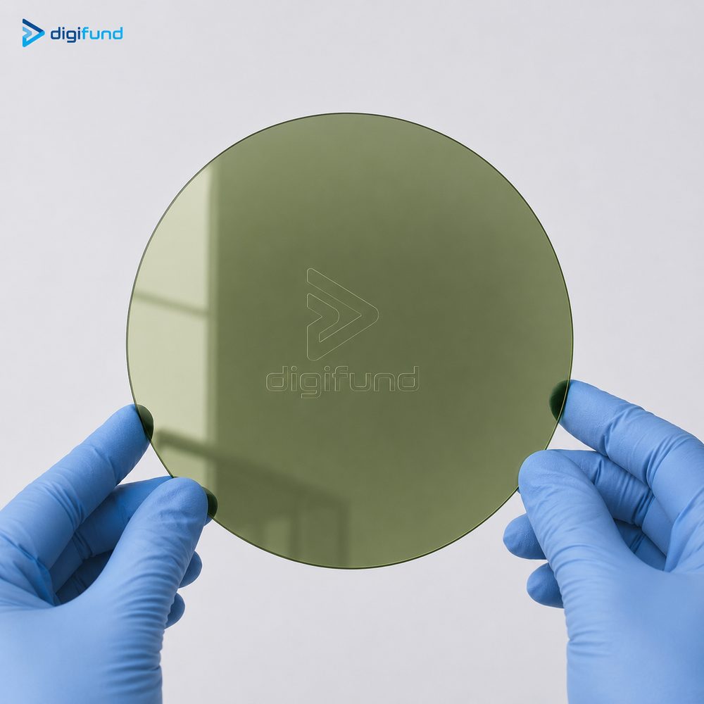
Digifund's SiC wafer range covers 4H-SiC and 6H-SiC polytypes, 2", 3", 4" and 6" sizes (8" as an option), N-type (nitrogen), semi-insulating HPSI and P-type, Prime – Research/Dummy grades, (0001) on-axis or 4° off-axis orientation, and 350 µm or 500 µm thickness. Representative items:
| Product | SKU | Polytype | Type | Size | Thickness | Orientation | Polish | Grade |
|---|---|---|---|---|---|---|---|---|
| SiC 3" HPSI Prime | DG-SiC-030001 | 4H-SiC | Semi-Insulating (HPSI) | 3" | 350 µm | — | — | Prime |
| SiC 3" N-type | DG-SiC-030002 | 4H-SiC | N-type (Nitrogen) | 3" | 350 µm | — | Single side | Prime |
| SiC 4" N-type | DG-SiC-040001 | 4H-SiC | N-type (Nitrogen) | 4" | 500 µm | Off-axis 4° | Double side | Prime |
| SiC 6" N-type | DG-SiC-060001 | 4H-SiC | N-type (Nitrogen) | 6" | 500 µm | — | — | Prime |
9. Specifications to send for a quote
For an accurate SiC substrate quote, send the following:
- Polytype (4H or 6H) and type: N-type, HPSI or P-type.
- Diameter (inch / mm), thickness and tolerance.
- Orientation: on-axis (0001) or off-axis (for example 4°), and the off-cut direction.
- Required resistivity range.
- Single- or double-side polish, Si-face or C-face, and whether an epi-ready surface is needed.
- Grade (Prime / Research / Dummy) and any MPD requirement.
- Flat style, quantity, intended use and required delivery date.
Frequently asked questions
How is a SiC wafer different from a silicon wafer?
SiC has a bandgap of about 3.2 eV (versus 1.12 eV for Si), a breakdown field about 10 times higher and roughly 2–3 times better thermal conductivity. SiC devices therefore handle higher voltage and temperature, suiting power electronics and RF. In return, SiC wafers are smaller and far more expensive.
Should I choose 4H-SiC or 6H-SiC?
Choose 4H-SiC for most uses: power devices, GaN-on-SiC and most device research, because 4H has a wider bandgap and higher electron mobility. 6H-SiC is mainly used when a process or research project specifically calls for it.
When do I need HPSI SiC instead of N-type?
Use HPSI (semi-insulating) for RF devices such as GaN HEMTs, where an insulating substrate reduces signal loss. Use N-type for vertical power devices such as MOSFETs and Schottky diodes, where current flows through the substrate.
What SiC wafer sizes does Digifund supply?
Digifund's range covers 2", 3", 4" and 6" (8" as an option), 4H and 6H polytypes, N-type, HPSI and P-type, at 350 µm or 500 µm thickness. Representative items are SiC 3" HPSI Prime, SiC 3" N-type, SiC 4" N-type and SiC 6" N-type.
Need SiC substrates for your project?
Send the polytype, conductivity type, diameter, thickness, orientation and quantity you need, and Digifund's technical team will advise and quote suitable SiC wafers.
Get technical advice View wafer catalog