



DIGIFUND VI Get a quote

01Silicon wafers & Substrates

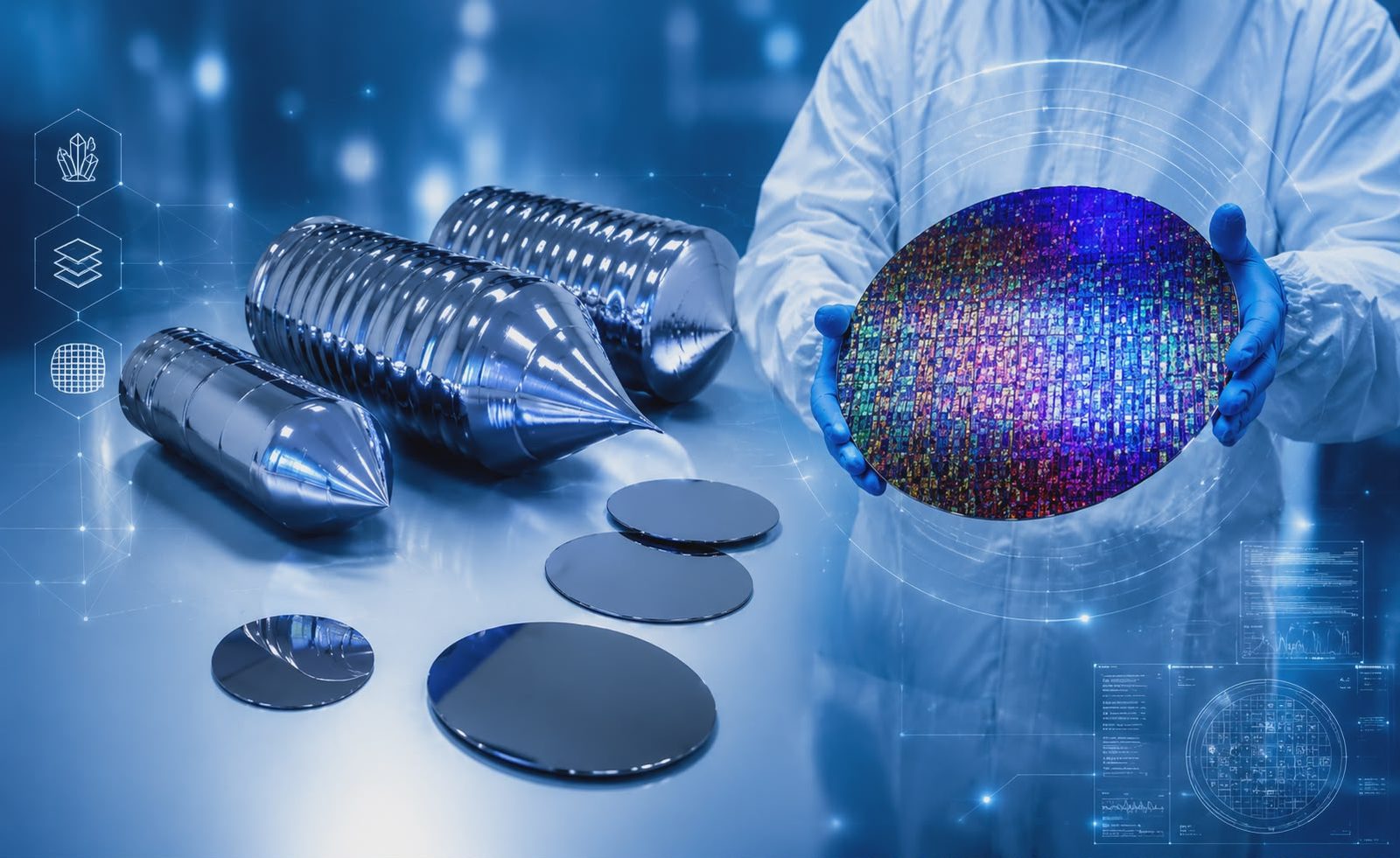
High-purity Silicon Wafer & Substrate

Digifund supplies high-quality silicon wafers to semiconductor makers worldwide, supporting advanced chip manufacturing with premium materials.

02Semiconductor fabrication materials

Semiconductor fabrication materials

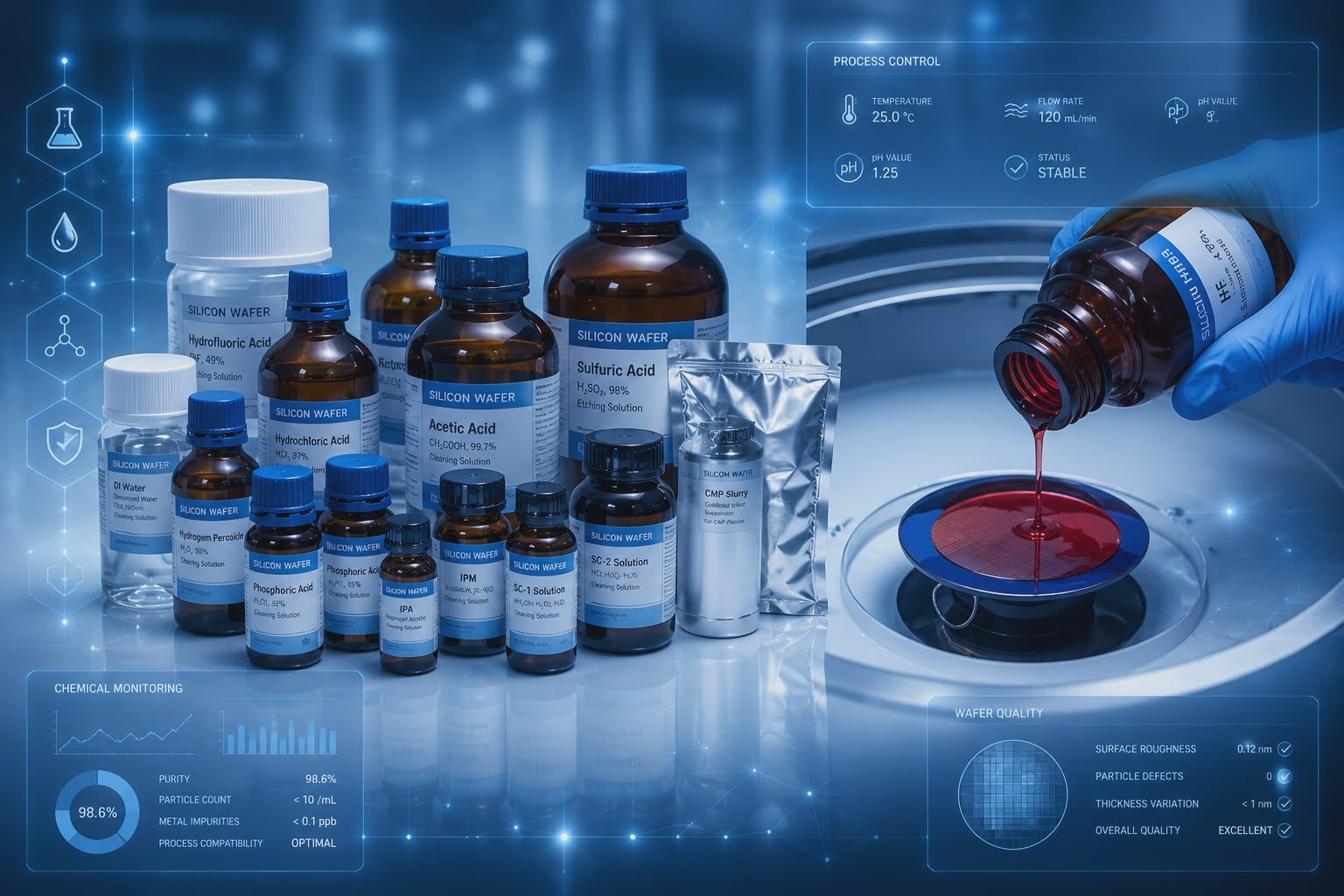
Photoresists, CMP materials, sputtering targets and wet-process chemicals for every lithography, etch, deposition and polishing step.

03Advanced packaging materials

Advanced packaging materials

Temporary bonding, carrier wafers, dicing consumables, plating chemistry, assembly and encapsulation materials for next-generation chip packaging.

04Cleanroom & Hi-tech Equipment

Cleanroom & hi-tech equipment

Fume hoods, wet benches, spin coaters, mask aligners, CVD, RIE and sputtering systems, and metrology for cleanrooms and semiconductor labs.

05Renewable energy materials & Equipment

Renewable energy materials & equipment

Photo-thermal-electrocatalytic reactors, fuel cell test stations, battery research equipment and nanomaterials for clean energy.

Key Applications / Domains

Key applications

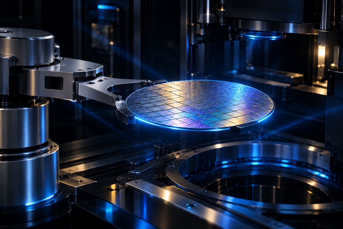
  • Robot arm lifting a silicon wafer inside a chip-making tool
    Semiconductor manufacturingSemiconductor manufacturing
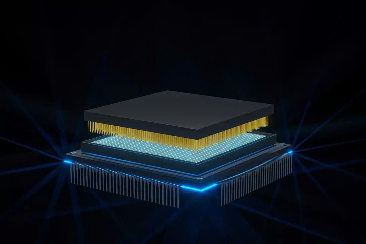
  • 3D model of advanced chip packaging layers
    Advanced packagingAdvanced packaging
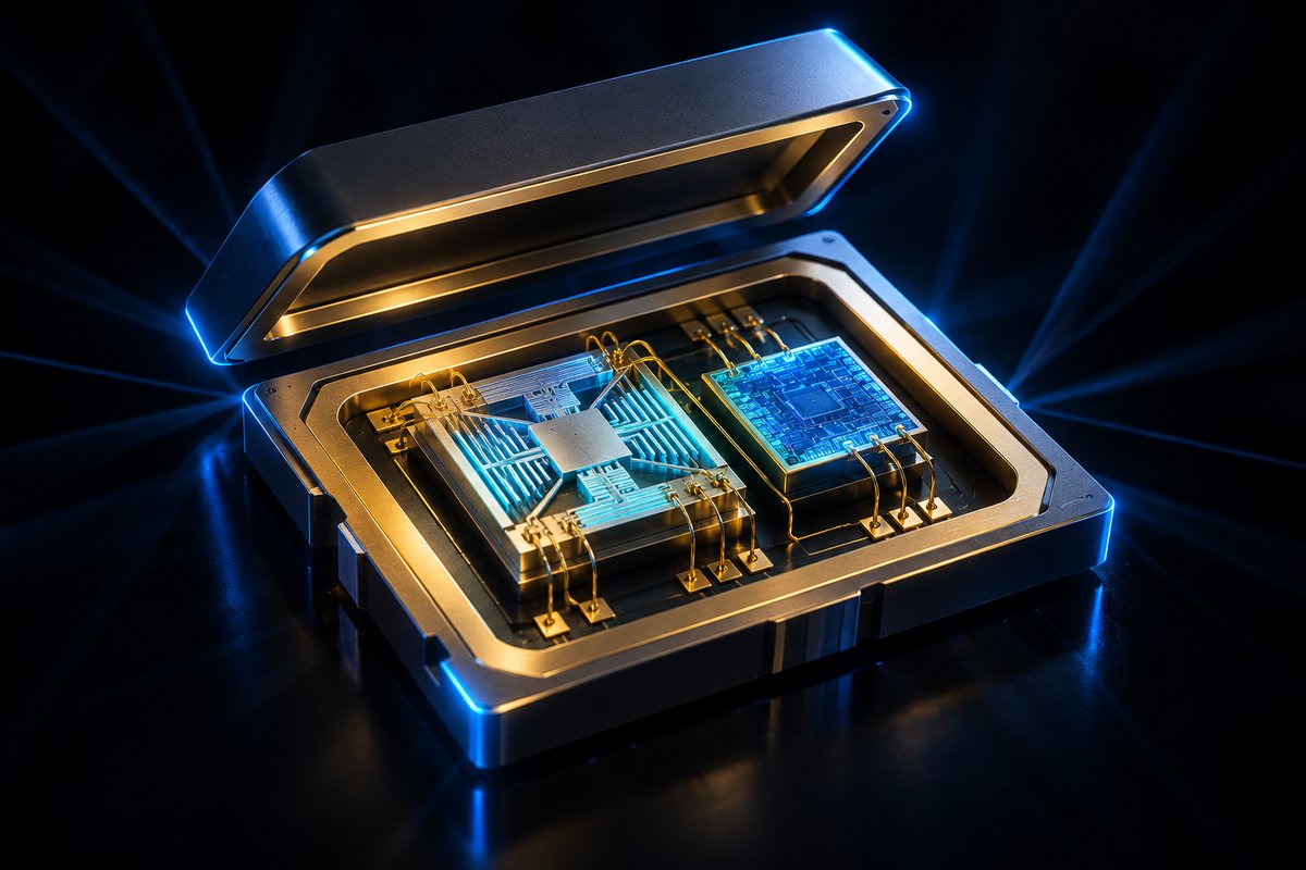
  • Open MEMS sensor package with a MEMS die and an ASIC
    MEMS & SensorsMEMS & sensors
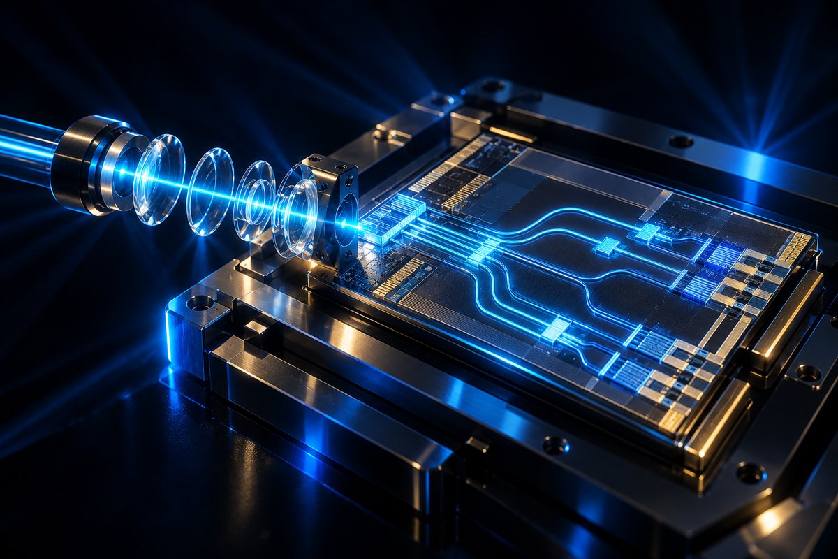
  • Laser beam through lenses into a silicon photonics chip
    PhotonicsPhotonics
  • GaN power device
    Power devicesPower devices

Silicon wafers are the base material for advanced semiconductor chips, electronics, sensor ICs and solar cells. DIGIFUND supplies high-quality silicon wafers, advanced materials and modern equipment to the semiconductor industry.

Semiconductor value chain

Where DIGIFUND fits in the semiconductor chip manufacturing chain

  1. 01

    Start

    Starting wafer

    Wafer

  2. 02

    Lithography

    Lithography

    Lithography materials

  3. 03

    Etch

    Etch & clean

    Wet clean chemicals

  4. 04

    Deposition

    Thin-film deposition

    Sputtering targets

  5. 05

    Polishing

    CMP polishing

    CMP materials

  6. 06

    Packaging

    Packaging

    Advanced packaging materials

  7. 07

    Final devices

    Finished chips

What we do

DIGIFUND's 3 core services

Three services that work together: from materials, to technical consulting, to custom fabrication.

  1. 01

    Semiconductor materials & equipment supply

    • Supplies for the entire chipmaking process.
    • Plentiful, reliable supply.
    View products
  2. 02

    Technical & technology consulting

    • A team of seasoned experts.
    • 24/7 technical support.
    Meet the team
  3. 03

    Custom fabrication services

    • EU-standard lab for chip fabrication.
    • Highly skilled, specialised engineers.
    Send request

Main product groups

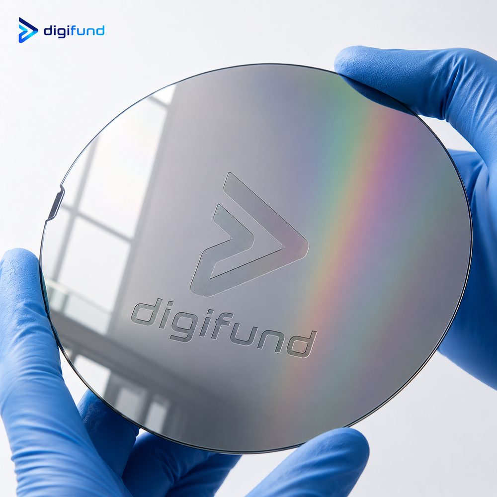
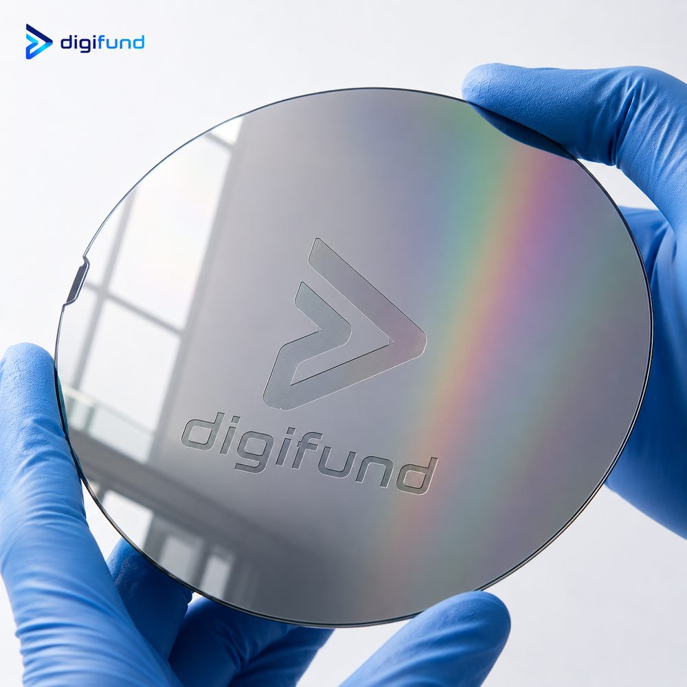
Polished silicon wafer in a technician's hand

01. Silicon Wafer & Substrate

High-purity silicon wafers, substrates and semiconductor materials for research and production of chips, ICs, sensors and solar cells.

  • Sizes from 2 to 12 inch (50–300 mm)
  • Quote on request
Product catalogue12 items
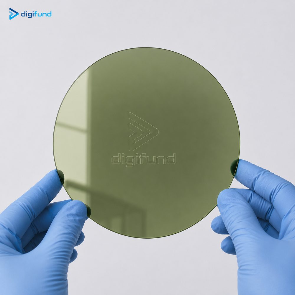
  • Silicon waferSiSiCSOISiN · Silicon nitride
  • Sapphire, AlN, GaAs, GaN, InP & other substratesSapphire (Al₂O₃)AlNGaAsGaNInPITO / Glass
  • Carrier wafersSilicon carrierGlass carrier
Quote on requestQuote
See all products in this group
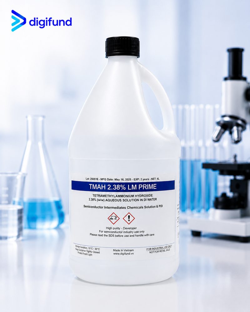
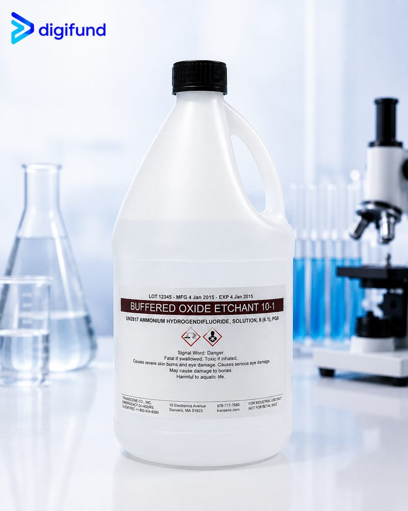
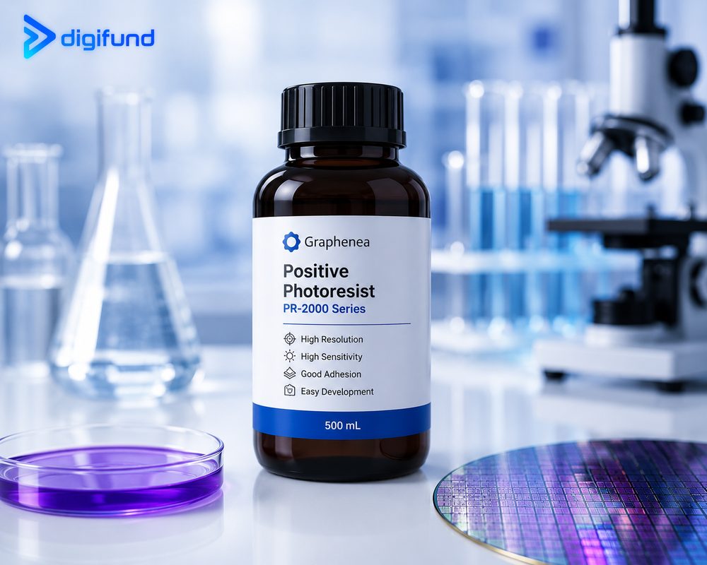
Positive photoresist for lithography

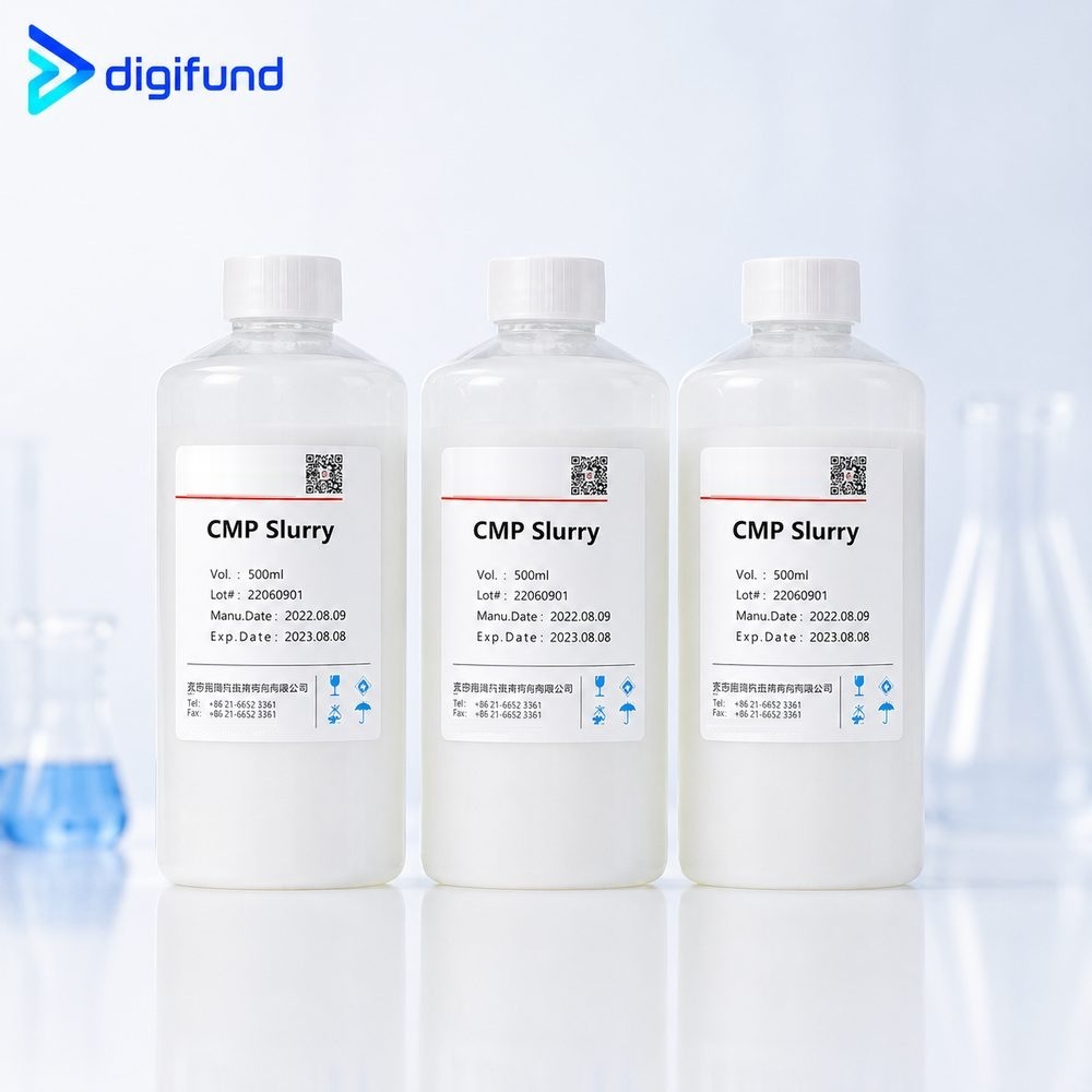
02. Semiconductor fabrication materials

Semiconductor fabrication materials for every lithography, CMP, thin-film deposition and wet-process step.

  • AZ, SU-8, N1400 and thick photoresists
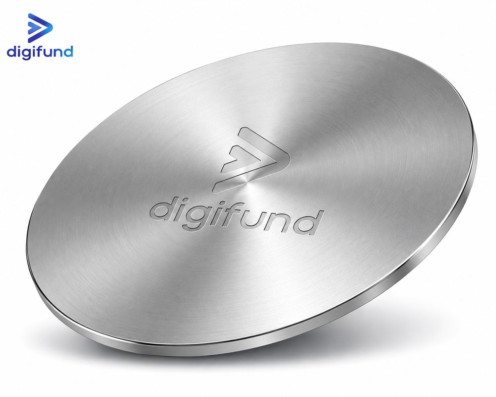
  • Sputtering targets and evaporation materials
Product catalogue17 items
  • Lithography materialsPhotoresist: AZ1512 · 1518 · 1502, N1400, SU-8, Thick PRDeveloper: AZ300-MIF, TMAH, MF-319HMDSStripper: SVC, PGMEAARC: DUV ARC, BARC
  • CMP materialsSlurry: Oxide, Cu, WPolishing padConditioner discCMP filter
  • Thin film materialsSputtering targetsEvaporation: pellets, wire
  • Wet process materialsIPAAcetoneNMPHFKOHH₃PO₄
Quote on requestQuote
See all products in this group
3D model of advanced chip packaging layers

03. Advanced packaging materials

Advanced packaging materials: from temporary bonding, carrier wafers and dicing to plating, assembly and encapsulation.

  • Temporary bonding & debonding
  • Underfill, silver epoxy, die attach film
Product catalogue12 items
  • Temporary bondingBonding adhesiveDebonding chemicals
  • Carrier solutionsSi / Glass carrier waferTemporary carrier wafer
  • Dicing consumablesUV dicing / back grinding tapeDicing blade
  • Plating & metallizationCu, Ni, Au plating chemistry
  • AssemblyUnderfillSilver epoxyDie attach filmConductive adhesive
  • EncapsulationMold compound
Quote on requestQuote
See all products in this group
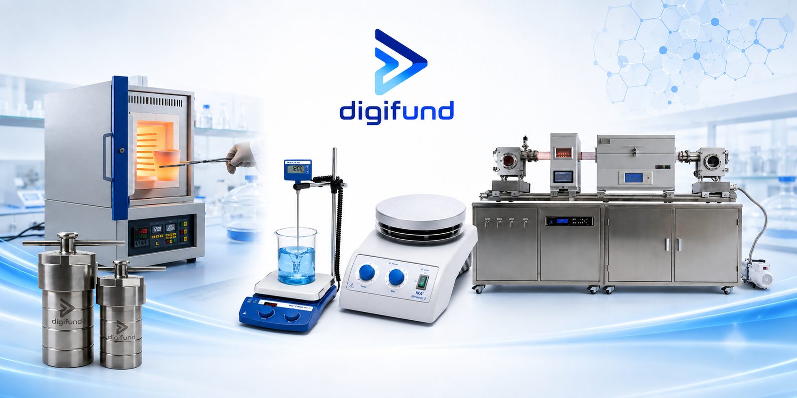
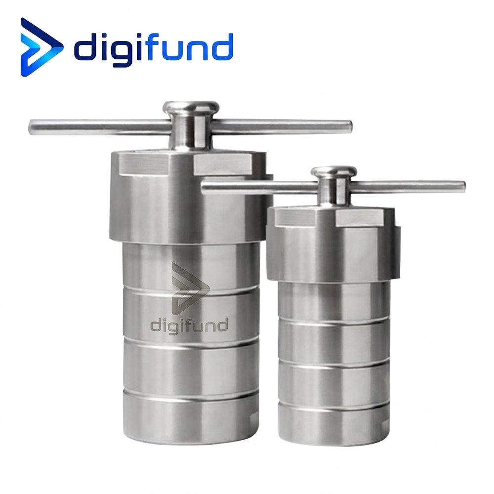
Digifund heating and laboratory equipment

04. Cleanroom & hi-tech equipment

Cleanroom & hi-tech equipment: cleanroom, semiconductor process, metrology and laboratory equipment for research institutes, universities and industry.

  • Spin coater, mask aligner, direct laser writer
  • CVD, RIE and sputtering systems
Product catalogue15 items
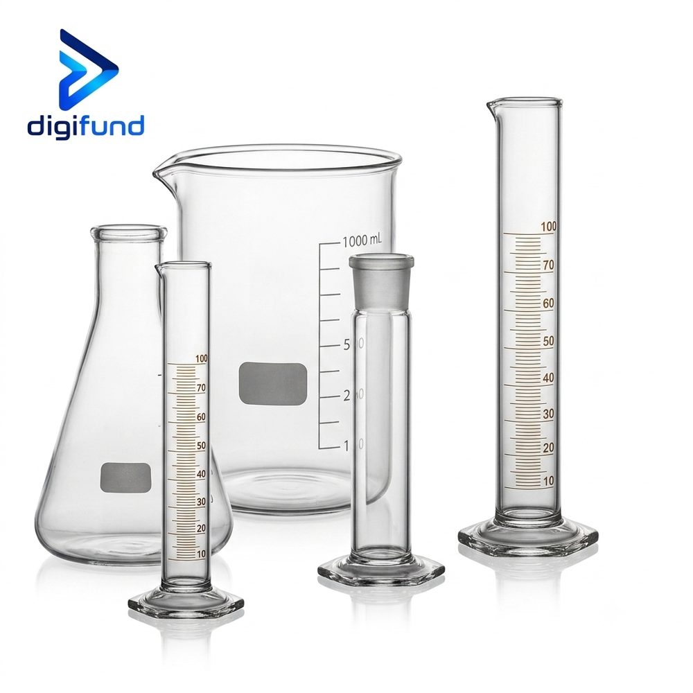
  • Cleanroom equipmentFume hoodWet benchGlasswareGloves + bunny suit
  • Semiconductor process equipmentSpin coaterMask alignerDirect laser writerCVDRIESputtering system
  • Metrology & characterizationOptical microscopeProfilometer
  • Laboratory equipmentVacuum systemGas deliveryProcess monitoring
Quote on requestQuote
See all products in this group
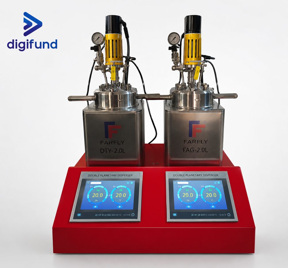
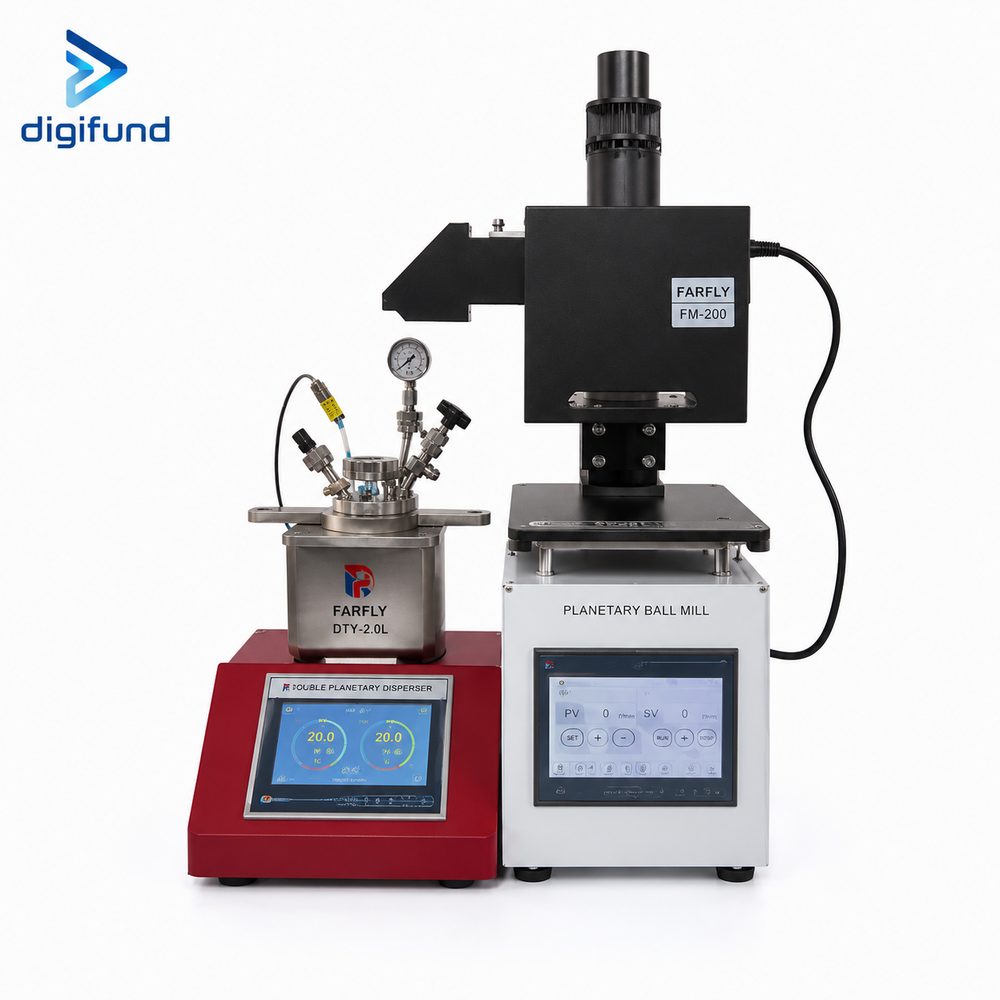
Photocatalytic reactor and accessories

05. Renewable energy materials & equipment

Renewable energy materials & equipment: catalytic reactors, fuel cells, energy storage and nanomaterials for clean energy.

  • Photo-thermal-electrocatalytic reactors
  • Nanomaterials: graphene, CNT, TiO₂
Product catalogue9 items
  • Solar energy & fuel cellPhoto-thermal-electrocatalytic reactorFuel cell test station
  • Energy storageBattery research equipmentAdvanced materials
  • NanomaterialsGraphene oxideMWCNTAu nanoparticlesTiO₂ P25TiO₂ anatase
Quote on requestQuote
See all products in this group

Advisory board

Advisors from CNRS (France), Gachon University (Korea) and Griffith University (Australia).

Collaboration & research

Digifund materials and equipment are used in photocatalysis and semiconductor fabrication research published in leading international journals.

Nature Energy cover
2026

Exploiting the insulator–metal transition of VO2 in photocatalytic methane conversion

Nature Energy 11, 613–622

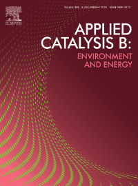
Applied Catalysis B: Environment and Energy cover
2025

Electricity-driven selectivity in the photocatalytic oxidation of methane to carbon monoxide with liquid gallium-semiconductor composite

Applied Catalysis B: Environment and Energy 363, 124834

Nature Communications cover
2024

Photocatalytic dihydroxylation of light olefins to glycols by water

Nature Communications 15.1, 8210

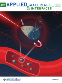
ACS Applied Materials & Interfaces cover
2024

Boosting gas-phase TiO2 photocatalysis with weak electric field strengths of volt/centimeter

ACS Applied Materials & Interfaces 16.12, 14852–14863

Case study Digifund products in real research projects Click to learn moreClick to collapse
01

Photocatalytic reaction systems for renewable energy

  • Photocatalysis
  • CH₄
  • VO₂
  • TiO₂
System layout: light source, reactor, electrochemistry and GC analysis
CH₄ conversion on VO₂ catalyst under UV light
Weak electric field effect in TiO₂ photocatalysis
02

Photocatalytic systems for solar cell applications

  • Thin-film solar cells
  • Reactor
Real reaction setup: light source, reactor and cooling
Photocatalysis integrated on a thin-film solar cell
03

Silicon wafers in micro/nano structure fabrication

IEMN, France · with a European research institute

  • p-Si
  • n-Si
  • SiNW
  • Lithography

p-Si wafers as substrates for p-n junctions

01p-Si wafer, the starting substrate
02SiNW etched with Ag⁺ ions, Ag⁺ removed with HNO₃, TiO₂ coated by ALD
03Cross-section SEM of the SiNW/TiO₂ p-n junction

n-Si wafers as substrates for microelectronics

01n-Si wafer, the starting substrate
02Direct laser lithography on the wafer
03After exposure, through development
04Placed in a vacuum chamber for dry etch

From grains of sand to silicon wafers, the backbone of the semiconductor industry. Digifund connects two key pillars of the future: semiconductors and clean energy.

  • 500+

    Products delivered

  • 20+

    Expert engineers

  • 50+

    Clients worldwide

  • 100%

    Quality assured

About Digifund

Founded 2023 · Ho Chi Minh City

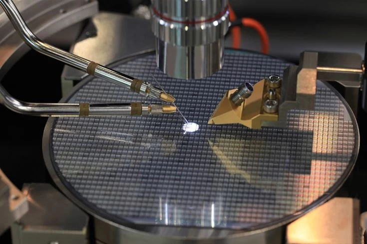
Semiconductor silicon wafer fab

Digifund is a trusted supplier of advanced materials and technical solutions for the semiconductor and renewable energy industries. Founded in 2023, we focus on connecting two key pillars of the future: semiconductors and clean energy.

We specialise in silicon wafers, substrates and essential high-quality materials for semiconductor research and production, supporting both lab-scale innovation and industrial manufacturing. Beyond materials, Digifund also supplies cleanroom and laboratory equipment, high-purity chemicals and consumables for high-tech industries.

  • ISO-standard quality assurance.
  • Full technical support on every order.
  • Industry-leading wafer specifications and purity standards.

Frequently asked questions

Learn more about silicon wafers on our semiconductor knowledge blog.

What is Digifund?

Digifund is a silicon wafer and semiconductor materials supplier in Vietnam. Digifund supplies silicon wafers (Si, SiC, GaAs, Sapphire, SOI), substrates, sputtering targets, chemicals and cleanroom equipment for the semiconductor industry, research and IC manufacturing.

Who supplies silicon / semiconductor wafers in Vietnam?

Digifund is a silicon and semiconductor wafer supplier in Vietnam, serving customers nationwide. Contact Digifund at digifund.vn, by phone +84 979 324 567 or by email semiconductor@digifund.vn.

Where can I buy silicon wafers in Vietnam?

You can buy silicon wafers in Vietnam through Digifund. Digifund supplies Si, SiC, GaAs, Sapphire and SOI wafers and substrates with quotes on request. Contact +84 979 324 567 or semiconductor@digifund.vn for advice.

Which wafers does Digifund supply?

Digifund supplies Si (silicon), SiC (silicon carbide), GaAs (gallium arsenide), Sapphire and SOI wafers, plus many other semiconductor substrates. See also: Types of silicon wafer.

Besides silicon wafers, what else does Digifund supply?

Digifund supplies five product groups: (1) silicon wafers and substrates; (2) semiconductor fabrication materials: photoresists, CMP materials, sputtering targets and wet-process chemicals; (3) advanced packaging materials: temporary bonding, carrier wafers, dicing consumables, plating chemistry, underfill, die attach film; (4) cleanroom and hi-tech equipment: fume hoods, wet benches, spin coaters, mask aligners, CVD, RIE and sputtering systems, and metrology; (5) renewable energy materials and equipment.

Where is Digifund and how do I get in touch?

Digifund is at 14th Floor, HM Town Building, 412 Nguyen Thi Minh Khai, Ban Co Ward, Ho Chi Minh City. Phone: +84 979 324 567. Email: semiconductor@digifund.vn.

Need materials or equipment for your next project?

Contact our team for specifications, quotes and custom orders. We reply within 24 hours.

Address

14th Floor, HM Town Building, 412 Nguyen Thi Minh Khai, Ban Co Ward, Ho Chi Minh City

Phone

+84 979 324 567

Email

semiconductor@digifund.vn

Social

Zalo · LinkedIn