
Contents
1. What is a silicon wafer?
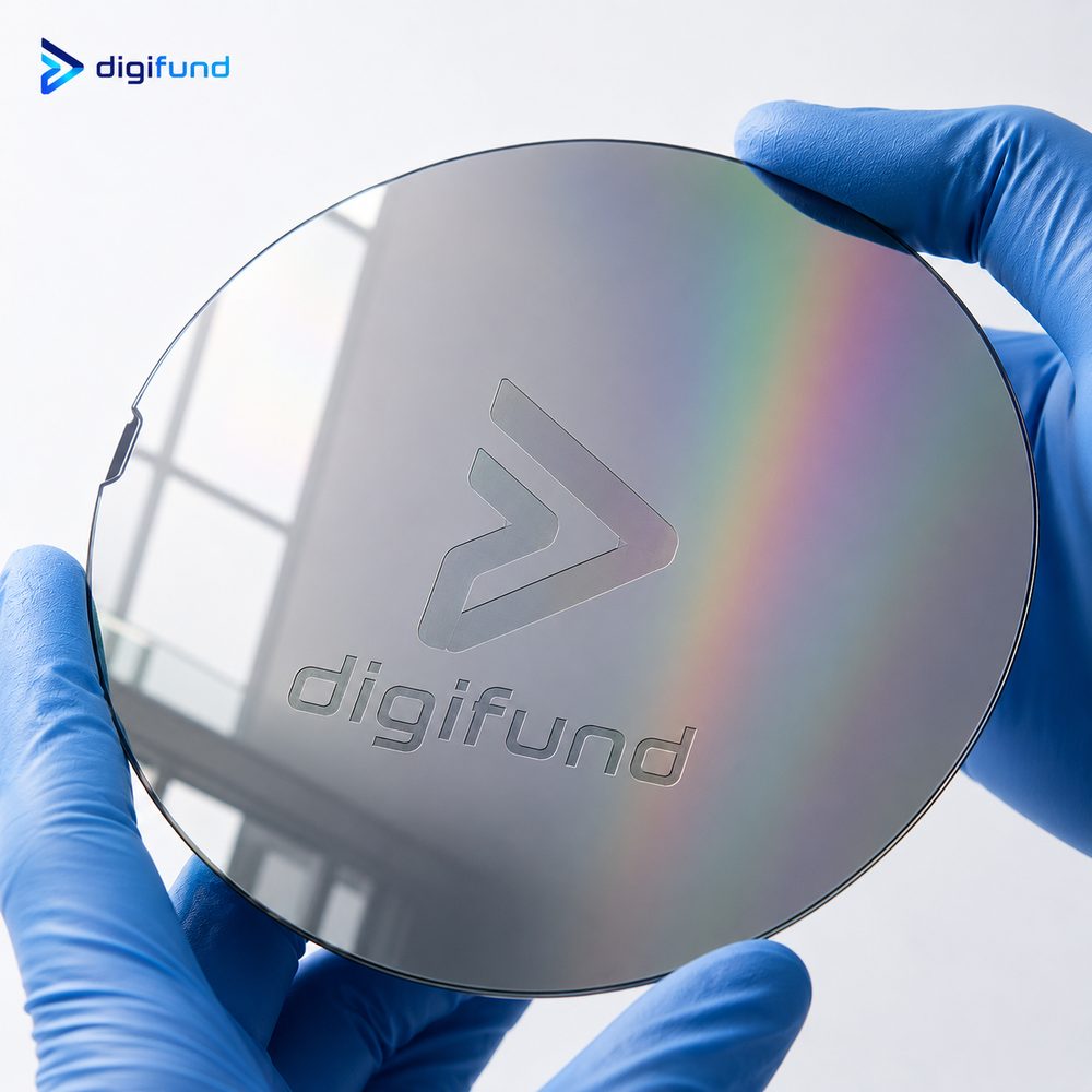
A silicon wafer (also called a silicon slice or silicon substrate) is a thin, round slice cut from a single-crystal silicon ingot of extremely high purity — typically above 99.9999999% ("9N"). It is the base material (substrate) on which millions, even billions, of transistors are built to form integrated circuits (ICs) and semiconductor chips.
Simply put, if the chip is the "brain" of every electronic device — from phones, computers and cars to satellites — then the silicon wafer is the physical foundation on which that brain is built. Without high-quality silicon wafers, the chip industry could not exist.
2. Structure and characteristics of a silicon wafer
Silicon wafers are made from silicon — the second most abundant element in the Earth's crust, found in quartz sand (SiO₂). However, semiconductor wafers require silicon that is highly pure with a perfect crystal structure. A high-quality silicon wafer has these characteristics:
- Extremely high purity: impurities are controlled to parts-per-billion (ppb) so they don't affect the chip's electrical properties.
- Single-crystal structure: the whole slice is one continuous crystal, oriented along a defined crystal plane (e.g. <100> or <111>).
- Ultra-flat, mirror surface: polished by chemical-mechanical planarization (CMP) to nanometer flatness, scratch-free.
- Uniform thickness: typically 275µm to 925µm depending on wafer diameter.
3. Manufacturing a silicon wafer: from sand to wafer
The journey turning grains of sand into a gleaming silicon wafer goes through several complex steps:
- Silicon refining: quartz sand (SiO₂) is reduced to metallurgical silicon, then purified into ultra-pure polysilicon.
- Growing the single-crystal ingot: polysilicon is melted and pulled into a large single-crystal ingot using the Czochralski (CZ) or Float Zone (FZ) method.
- Slicing: the ingot is cut into thin slices with a diamond wire saw.
- Lapping & polishing: each slice is lapped flat then chemical-mechanically polished (CMP) to a mirror finish.
- Cleaning & inspection: wafers are cleaned in a cleanroom and inspected for defects before packaging.
4. Sizes and types of silicon wafer
Silicon wafers are produced in various diameters. The larger the size, the more chips can be cut from each wafer, lowering production cost.
| Diameter | Metric | Common uses |
|---|---|---|
| 2 inch | 50,8 mm | Research, R&D, LED, new materials |
| 4 inch | 100 mm | Sensors, MEMS, power electronics |
| 6 inch | 150 mm | Power electronics, SiC, LED |
| 8 inch | 200 mm | Analog ICs, sensors, MEMS |
| 12 inch | 300 mm | CPUs, GPUs, high-end DRAM/Flash memory |
Besides silicon (Si), the market also offers compound semiconductor wafers and other substrates such as SiC, GaAs, Sapphire, InP and SOI. See details in Types of Silicon Wafer.
5. Applications of silicon wafer
Silicon wafers are the base material for most modern electronic devices:
- Processors & memory: CPUs, GPUs, RAM, AI chips in computers and phones.
- Sensors & MEMS: image, acceleration and pressure sensors, microelectromechanical systems.
- Power electronics: EV control modules, renewable energy (especially SiC wafers).
- Solar cells: mono/poly crystalline silicon slices are the core of photovoltaic cells.
- Photonics & LED: substrates for light-emitting diodes and semiconductor lasers.
More detail in Applications of Silicon Wafer in semiconductors, energy and sensors.
6. Where to buy silicon wafers in Vietnam?
Digifund is a supplier of high-purity silicon wafers, substrates and semiconductor materials in Vietnam. We offer a wide range of Si, SiC, GaAs, Sapphire, InP and SOI wafers in various sizes and specifications, serving research institutes, universities and domestic manufacturers.
7. How to read a wafer specification sheet
On a quotation or a lot inspection report you will meet a dense specification line like this:
Prime CZ-Si, 4", (100), P-type (B), 1–10 Ω·cm, SSP, 525 ± 25 µmDecoding it piece by piece:
| Field | Meaning |
|---|---|
| Prime | Top grade, tightest tolerances. Test and Dummy grades are cheaper |
| CZ-Si | Grown by the Czochralski method. FZ means Float Zone: purer and dearer |
| 4" | Nominal diameter, equivalent to 100 mm |
| (100) | The crystal plane parallel to the wafer surface |
| P-type (B) | Boron doped, majority carriers are holes. N-type uses phosphorus, carriers are electrons |
| 1–10 Ω·cm | Resistivity band. The narrower the band, the higher the price |
| SSP | Single side polished. DSP means double side polished and costs more |
| 525 ± 25 µm | Nominal thickness and tolerance |
You may also encounter TTV (total thickness variation), bow and warp — three flatness metrics that matter when your process has a shallow depth of focus. The flat or notch on the wafer edge marks crystal orientation and doping type.
8. Handling and storing wafers
A polished wafer is among the cleanest surfaces an ordinary lab ever handles. A single fingerprint can ruin a fabrication run, because salts and oils from skin diffuse into the silicon during high-temperature steps.
- Handle only with soft-tipped wafer tweezers or a vacuum pen. Always contact the edge, never the polished face.
- Wear clean nitrile gloves; avoid powdered latex.
- Store in a proper cassette or coin box, kept dry and out of strong light.
- Never stack wafers face to face in direct contact.
- On an SSP wafer the matte side identifies the back — the polished face is mirror-like.
- Wafers left in air grow a native oxide; if your process is sensitive, include a dilute HF strip immediately before use.
Frequently asked questions
How thick is a wafer, and why not thinner?
Standard thickness scales with diameter, from around 275 µm at 2 inch up to 725 µm at 8 inch. The reason they are not thinner is mechanical strength: larger wafers need more thickness to avoid warping or breaking during handling and high-temperature processing.
What is the flat on the wafer edge for?
The flat marks crystal orientation, letting you align masks correctly and telling you which way the wafer will cleave. The relative position of the primary and secondary flats also encodes doping type. Larger-diameter wafers use a notch instead of a flat to waste less area.
Can silicon wafers be reused?
Test and dummy wafers can be repolished and reused several times, losing a little thickness each cycle. Wafers that have carried devices are not reused for production, but still serve as furnace fillers or student practice pieces. In a lab, reusing test wafers for calibration is a meaningful saving.
Need help choosing the right silicon wafer?
Digifund's engineers help you pick the right wafer type, size and specifications for your semiconductor project.
View Silicon Wafer catalog Request a quote