
Contents
- What is CMP and why is it needed?
- Mechanism: chemistry plus mechanics
- Main CMP steps in chip fabrication
- CMP slurry: composition and selection
- CMP pads: hard, soft and stacked
- Conditioners, filters and accessories
- Process parameters and metrics
- Post-CMP cleaning
- CMP consumables Digifund supplies
- Specifications to send for a quote
1. What is CMP and why is it needed?
CMP (chemical mechanical planarization, or chemical mechanical polishing) presses a wafer face-down onto a rotating pad while a liquid of abrasive particles and chemicals, the slurry, is fed continuously onto the pad. The chemistry softens or oxidises the surface layer, and the abrasive and pad sweep it away. The result is a surface that is planarised across the whole wafer, not just locally polished.
Every deposition and etch step adds topography. Without planarisation, upper layers would fall outside the depth of focus of the lithography tool and metal lines would break over steps. CMP is therefore mandatory for multi-level metal chips, and it is also how copper wiring is formed in the damascene process. Depth-of-focus limits are covered in the photolithography process article.
2. Mechanism: chemistry plus mechanics
The material removal rate (MRR) is commonly approximated by the Preston equation: MRR ≈ Kp · P · V, where P is the down-force pressure, V the relative velocity between wafer and pad, and Kp a coefficient lumping together slurry, pad and material effects. Higher pressure or speed removes material faster but also tends to increase scratches and hurt uniformity.
Why does CMP planarise? High points see higher local pressure, so they are removed faster than low areas. The chemistry decides which material is removed quickly and which acts as a stop layer, the slurry's selectivity.
3. Main CMP steps in chip fabrication
Each application needs its own slurry – pad pairing. The table summarises common systems; exact formulations vary by supplier and process.
| CMP step | Typical abrasive | Chemistry | Goal / stop layer |
|---|---|---|---|
| ILD oxide (interlayer dielectric) | Silica (fumed / colloidal) | Alkaline, pH ≈ 10–11 | Planarise oxide, timed removal |
| STI (shallow trench isolation) | Ceria (CeO₂) or silica | With selectivity additives | Remove oxide, stop on nitride (Si₃N₄) |
| Tungsten (W plug) | Silica or alumina | Acidic, with oxidiser (often H₂O₂) | Remove excess W, stop on oxide / barrier |
| Copper (Cu damascene) | Colloidal silica, low loading | Oxidiser, complexing agent, corrosion inhibitor (e.g. BTA) | Step 1 removes Cu, stops on barrier; step 2 removes barrier (Ta/TaN) |
| Polysilicon | Silica | Alkaline | Planarise poly, stop on oxide |
| Silicon wafer polishing | Colloidal silica | Alkaline | Stock removal, then final polish to a mirror surface |
Copper must be protected from corrosion and dishing during polishing, so copper slurries are always more complex than oxide slurries. Silicon wafer polishing is the last step of wafer manufacturing and sets the roughness and flatness you see on a datasheet; see what is a silicon wafer.
4. CMP slurry: composition and selection
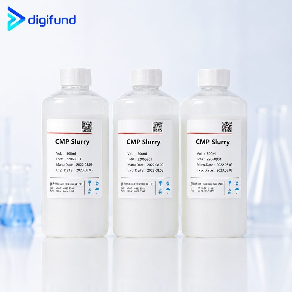
A CMP slurry has these main components:
- Abrasive — colloidal silica, fumed silica, ceria or alumina, typically tens to a few hundred nanometres. More uniform particles with fewer oversized ones mean fewer scratches.
- Solids loading — in wt%; oxide slurries are usually more concentrated than copper slurries.
- pH and buffer — control reaction rate and particle stability.
- Oxidiser — for metal slurries (W, Cu), usually H₂O₂, added just before use.
- Complexing agents, corrosion inhibitors, surfactants — tune selectivity, limit dishing and reduce defects.
To choose a slurry, start from the material to remove and the material to stop on, then the target removal rate and the acceptable defect level. A few handling notes:
- Do not let slurry freeze or overheat; particles can agglomerate irreversibly.
- Shake or stir before use, as particles settle over time.
- Slurry mixed with oxidiser has a limited pot life; mix only what you need.
- Use point-of-use filters to catch agglomerates that cause scratches.
- Follow the shelf life and storage conditions on each lot's label.
5. CMP pads: hard, soft and stacked
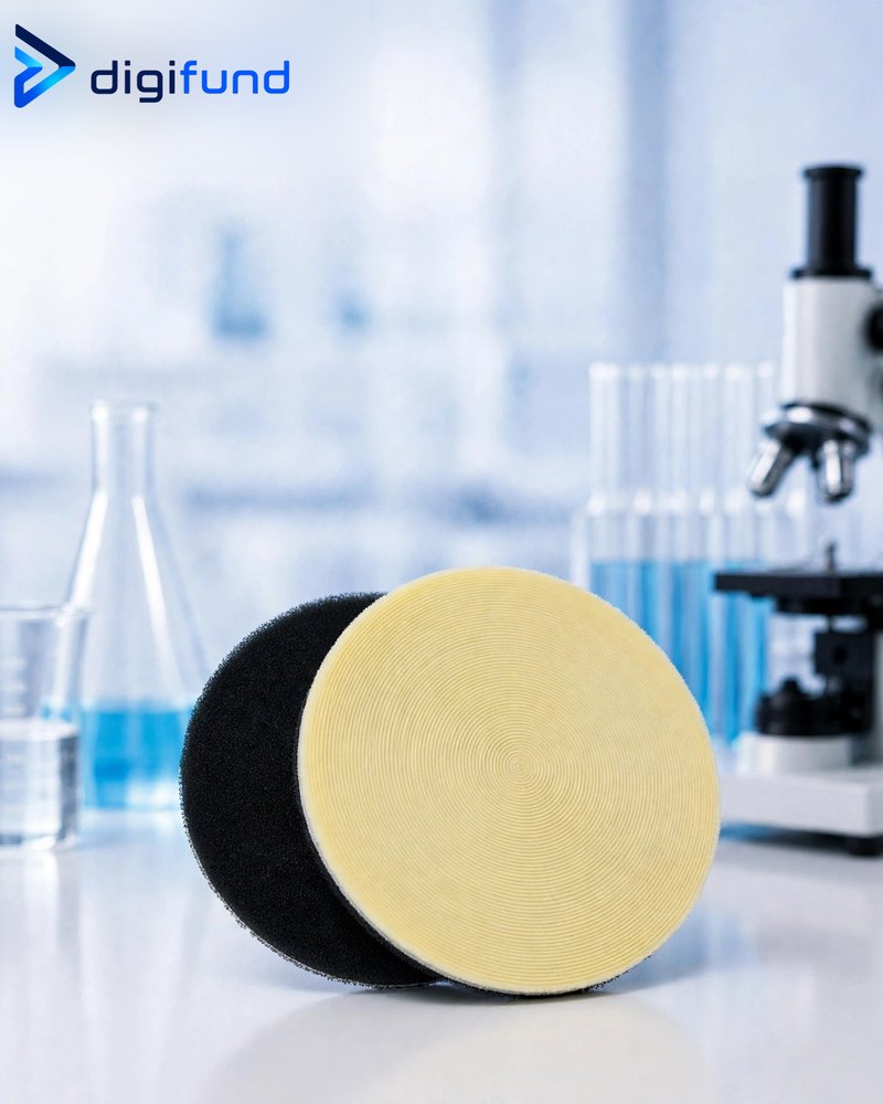
The pad holds and distributes slurry and transmits pressure to the wafer. Its stiffness decides how it "sees" surface topography:
| Hard pad | Soft pad | |
|---|---|---|
| Material | Cast microporous polyurethane | Poromeric (polyurethane-impregnated felt) |
| Strength | Good planarisation, conforms little | Low scratching, smooth finish |
| Used for | Main removal steps: oxide, W, Cu | Final polish, buffing, final silicon wafer polish |
A stacked pad (a hard pad laminated on a soft sub-pad) is the compromise: the hard top keeps local planarity while the soft base lets the pad follow whole-wafer curvature for better uniformity. Grooves on the pad surface (XY, concentric K-groove…) distribute fresh slurry and carry spent slurry and debris away. Pad size must match the CMP tool's platen.
6. Conditioners, filters and accessories
- Pad conditioner — a diamond disc (plated or CVD) that lightly abrades the pad to reopen pores clogged by slurry and debris ("glazing"). Without conditioning, removal rate decays wafer after wafer.
- Slurry filters — depth filters of roughly 0.5–10 µm that stop agglomerates before they reach the pad.
- Retaining ring — holds the wafer in the polishing head and also affects edge uniformity; a wear part.
- PVA brushes — used in post-CMP cleaning.
7. Process parameters and metrics
The ranges below are common reference values for 200 / 300 mm wafer CMP tools; the actual operating point must be tuned for the specific tool, slurry and pad.
| Parameter | Reference range | Effect |
|---|---|---|
| Down-force | ~1–6 psi (~7–40 kPa) | Raises MRR; too high causes scratches, dishing |
| Platen / head speed | ~30–120 rpm | Raises MRR, affects uniformity |
| Slurry flow | ~100–300 mL/min | Too little runs dry and hot; too much wastes slurry |
| Pad temperature | Monitored, typically a few tens of °C | Changes chemical reaction rate |
Metrics used to judge a CMP result:
- MRR — removal rate in nm/min or Å/min.
- WIWNU — within-wafer non-uniformity, %.
- Dishing (recess in wide metal lines) and erosion (dielectric loss in dense line arrays).
- Selectivity — removal-rate ratio between the target material and the stop layer.
- Defects — scratches, particles, corrosion, organic residue.
8. Post-CMP cleaning
After CMP, the wafer carries abrasive particles, metal ions and inhibitor residue. It must be cleaned immediately, before slurry dries on. A typical sequence is PVA brush scrubbing with a cleaning chemistry (dilute alkaline for oxide, mildly acidic or complexing chemistry for Cu), DI water rinse, optional megasonic, then spin dry. General cleaning chemistry and wafer handling are covered in silicon wafer cleaning (RCA).
9. CMP consumables Digifund supplies
Digifund supplies CMP consumables for fabs and labs in Vietnam:
| Group | Options |
|---|---|
| CMP slurries | Silica slurries for oxide, copper (Cu) and tungsten (W) |
| CMP pads | Hard polyurethane / soft poromeric pads; single layer or stacked with sub-pad; XY, K-groove or concentric grooves; sized for 200 / 300 mm CMP tools; for oxide, Cu, W, Si |
| CMP accessories | Diamond conditioner discs (plated / CVD), 0.5–10 µm slurry filters, retaining rings, post-CMP PVA brushes |
10. Specifications to send for a quote
- Material to polish and the stop layer (for example oxide on nitride, W on oxide, Cu on Ta/TaN, bare Si wafer).
- CMP tool or polisher in use, platen diameter and wafer / sample size.
- Target removal rate and roughness, flatness and defect requirements.
- Pad type (hard / soft / stacked), groove pattern, and whether a pressure-sensitive adhesive backing is needed.
- Current slurry (if you need an equivalent) and monthly quantity.
- Accessories needed: conditioners, filters, retaining rings, PVA brushes.
Frequently asked questions
How is CMP different from ordinary mechanical polishing?
Mechanical polishing relies on abrasives alone and tends to leave scratches and subsurface damage. CMP combines chemistry that softens or oxidises the surface with very fine abrasives, so it planarises the whole wafer and leaves a nanometre-smooth, low-defect surface.
Should I use silica or ceria slurry for oxide CMP?
Alkaline silica slurry is the common, easy-to-use choice for ILD oxide. Ceria slurry gives high oxide removal at low particle loading and can reach high oxide-to-nitride selectivity, so it is often used for STI. The final choice depends on the stop layer and the process's defect requirements.
When should I use a hard pad and when a soft pad?
Hard polyurethane pads deform little and planarise well, so they are used for main removal and planarisation. Soft poromeric pads conform more and scratch less, so they are used for final polish, buffing or final silicon wafer polishing. A hard pad stacked on a soft sub-pad balances local planarity and whole-wafer uniformity.
Which CMP consumables does Digifund supply?
Digifund supplies CMP slurries for oxide, copper and tungsten, hard polyurethane and soft poromeric pads (single layer or stacked with sub-pad, XY, K-groove or concentric grooves, sized for 200 / 300 mm tools), and accessories such as diamond conditioner discs, 0.5–10 µm slurry filters, retaining rings and post-CMP PVA brushes.
Need CMP slurry or pads for your process?
Send the material to polish, the stop layer, your CMP tool and wafer size, and Digifund's technical team will recommend a matching slurry – pad pair and send a quote.
Get technical advice View fabrication materials