
Contents
1. What is photoresist?
Photoresist is a light-sensitive polymer film coated onto a wafer, usually by spin coating. When it is exposed through a mask, the exposed areas change their solubility in the developer; after development, the remaining resist acts as a mask for etching, ion implantation, plating or lift-off. The whole sequence is explained in the photolithography process.
2. Positive vs negative photoresist
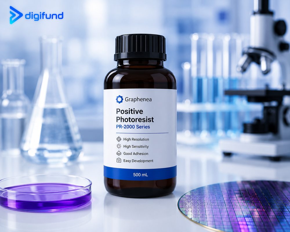
With a positive photoresist, exposed areas become soluble and are removed by the developer, so the pattern on the wafer matches the mask. With a negative photoresist, exposed areas crosslink and stay, so the pattern is the inverse of the mask.
| Criterion | Positive resist | Negative resist |
|---|---|---|
| Exposed area | Dissolves in the developer | Remains after development |
| Pattern vs mask | Same as the mask | Inverse of the mask |
| Examples Digifund supplies | AZ1512, AZ1518, AZ1502 | N1400, SU-8 |
| Typical developer | TMAH-based alkaline developer | Depends on the resist; SU-8 uses a PGMEA-based solvent |
| Strengths | Good dimension control, easy to strip | Durable patterns, thick layers, lift-off profiles |
The AZ 1500 series (AZ1512, AZ1518, AZ1502) are widely used positive resists for labs; they differ mainly in viscosity and therefore in the film thickness obtained at a given spin speed. A negative resist such as N1400 is often chosen when the next step is metal lift-off or when the pattern must survive harsher processing. Spin curves and bake and exposure conditions are given in each product datasheet.
3. SU-8 and thick resists
SU-8 photoresist is an epoxy-based, chemically amplified negative resist exposed in the near UV (i-line, 365 nm). In a single coat it can range from below 1 µm to hundreds of µm depending on viscosity, with near-vertical sidewalls and high aspect ratios. That is why SU-8 is widely used for MEMS, microfluidic moulds and permanent structures.
- It needs a post-exposure bake to complete crosslinking.
- It is developed in a PGMEA-based solvent, not in TMAH developer.
- Once fully crosslinked, SU-8 is very hard to strip; plan ahead if the layer must be removed.
Thick photoresists (Thick PR) cover films of several µm and above, used as plating moulds (bumps, copper pillars), deep-etch masks or over strong surface topography. Thick films need longer bake and development times and a higher exposure dose than thin films.
4. How to choose a photoresist
- Exposure wavelength. The resist must be sensitive at the wavelength your tool emits. Mask aligners use mercury lamps with g-line, h-line and i-line emission; laser writers usually use a single wavelength in the 375–405 nm range; DUV lithography needs dedicated 248 nm or 193 nm resists.
- Resolution. The smallest feature depends on both resist and tool. Thinner resist generally resolves smaller features; with a contact mask aligner the practical limit is usually around the micrometre level.
- Film thickness. Choose it for the next step: thick enough to survive dry etching, clearly thicker than the metal for lift-off, or as tall as the structure for plating moulds and SU-8.
- Downstream process. Wet etch, dry etch, lift-off, plating and permanent structures each favour different resists (see the positive/negative table above).
- Chemical compatibility. Developer and stripper must match the resist: positive resists use TMAH developer, SU-8 uses a solvent developer. Choose the whole set together to avoid process drift.
| Exposure line | Wavelength | Typical use |
|---|---|---|
| g-line | 436 nm | Mercury lamp, mask aligner |
| h-line | 405 nm | Mercury lamp, some laser writers |
| i-line | 365 nm | Mercury lamp, i-line steppers, SU-8 |
| KrF (DUV) | 248 nm | Excimer laser, needs DUV resist and usually ARC |
| ArF (DUV) | 193 nm | Excimer laser, advanced manufacturing |
5. The lithography chemistry Digifund supplies
Digifund supplies every material group needed for a complete lithography process, listed under "Lithography materials" in the semiconductor fabrication materials group:
| Group | Products | Role |
|---|---|---|
| Positive photoresists | AZ1512, AZ1518, AZ1502 | Micro-patterning, wet and dry etch masks |
| Negative photoresist | N1400 | Inverse patterns, lift-off |
| SU-8 | SU-8 | Thick, high-aspect-ratio structures, MEMS, microfluidic moulds |
| Thick photoresist | Thick PR | Plating moulds, deep etch, strong topography |
| Developers | AZ300-MIF, TMAH 2.38%, MF-319 | Developing positive resists; TMAH-based, metal-ion-free |
| Adhesion promoter | HMDS | Makes Si/SiO2 surfaces hydrophobic so the resist adheres |
| Strippers | SVC series, PGMEA | Removing resist after lithography; PGMEA is also used for rinsing and edge-bead removal |
| Anti-reflective coatings | DUV ARC, BARC | Reducing substrate reflection and standing waves, especially in DUV lithography |
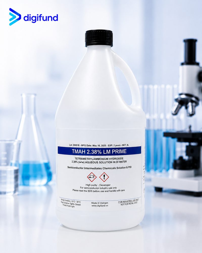
TMAH 2.38% is the industry-standard developer concentration for positive resists. Metal-ion-free (MIF) developers are preferred in semiconductor processing because they leave no sodium or potassium ions on the wafer.
6. Matching tools: spin coater, mask aligner
Chemicals give stable results only with the right tools. Digifund also supplies spin coaters for uniform resist coating, mask aligners and direct laser writers for exposure, plus fume hoods and wet benches for developing and stripping. See cleanroom & lab equipment. If you need wafers to run the process, see silicon wafers & substrates.

7. Storage, handling and safety
- Storage: keep resist in closed bottles, away from light and heat, at the temperature on the datasheet; some types need refrigeration. Let the bottle reach room temperature before opening so moisture does not condense into the resist.
- Shelf life: resists have a limited shelf life; sensitivity and viscosity drift over time. Mark the opening date and use stock first in, first out.
- Work lighting: handle resist under yellow (UV-filtered) light to avoid unintended exposure.
- Flammable solvents: resists and PGMEA contain flammable organic solvents; use them in a fume hood, away from ignition sources.
- TMAH is toxic: TMAH developer is toxic on skin contact, even when dilute. Always wear chemical-resistant gloves, goggles and a lab coat; rinse with plenty of water immediately after contact.
- SDS and waste: read the safety data sheet (SDS) before use and dispose of solvent and developer waste under hazardous-waste regulations.
Wafers must be clean and dry before HMDS and resist coating; the cleaning sequence is covered in RCA wafer cleaning.
8. How to request a quote
For Digifund to propose the right product and quote accurately, send the following:
- Product name (for example AZ1518, SU-8) or the resist type you want (positive, negative, thick).
- Target film thickness and smallest feature size.
- Exposure tool and wavelength (mask aligner, laser writer, i-line, DUV...).
- Substrate type and wafer size.
- The step after lithography: wet etch, dry etch, lift-off, plating or permanent structure.
- Quantity, bottle size, and any developer, HMDS, stripper or ARC you need with it.
- Delivery address and the documents you need, such as SDS or datasheet.
Send your request through the contact form, by email to semiconductor@digifund.vn or by phone on +84 979 324 567.
Frequently asked questions
Does Digifund supply photoresist in Vietnam?
Yes. Digifund supplies positive photoresists (AZ1512, AZ1518, AZ1502), negative photoresist (N1400), SU-8 and thick resists, together with developers, HMDS, strippers and anti-reflective coatings for labs and fabs in Vietnam. Send your process details to get a quote.
Should I choose a positive or a negative photoresist?
Positive resists such as the AZ 1500 series are the default for wet etch, dry etch and most micro-patterning because critical dimensions are easy to control and the resist strips easily. Negative resists suit durable patterns, thick layers or lift-off profiles. The final choice depends on your mask polarity, exposure tool and the next process step.
What developer does SU-8 use?
SU-8 is an epoxy-based negative resist and is normally developed in a PGMEA-based solvent developer, not in the TMAH developers used for positive resists. Once crosslinked, SU-8 is very hard to strip, so it is usually used as a permanent structure or a mould.
What information should I send to get a photoresist quote?
Send the product name or resist type, target film thickness and smallest feature size, your exposure wavelength, substrate type, the process after lithography, quantity and bottle size, and any matching developer or stripper you need.
Need photoresist and lithography chemicals in Vietnam?
Send the resist name or a description of your process, your exposure tool and target thickness. Digifund's technical team will propose a matching resist, developer and supporting chemicals with a quote.
Request a quote View chemicals & supplies